Experimental realization of two-dimensional Dirac nodal line fermions in monolayer Cu2Si
2018年01月23日
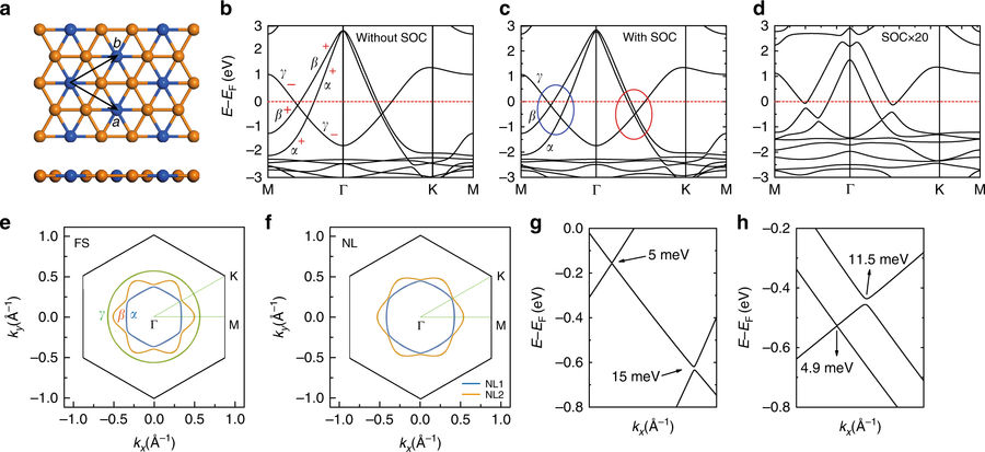
Figure 1 Atomic and band structures of free-standing Cu2Si. a Top and side view. The orange and blue balls represent Cu and Si atoms, respectively. b, c Calculated band structures of Cu2Si without and with spin-orbit coupling (SOC), respectively. The vertical axis E-E F corresponds to -E B, where E B is the binding energy. For simplicity, we label the three bands that cross the Fermi level α, β, and γ, respectively. The parity of mirror reflection symmetry for each band is labelled plus and minus signs in b. The zoom-in band structures in the blue and red ellipses are shown in g, h. d Band structure of Cu2Si after artificially increasing the intrinsic SOC by 20 times. e Fermi surface of Cu2Si without SOC. The blue, orange, and green lines correspond to bands α, β, and γ, respectively. f Momentum distribution of the nodal loops: NL1 (blue) and NL2 (orange). g, h Zoom-in band structures in the blue and red ellipses in c, which clearly show the SOC-induced gaps
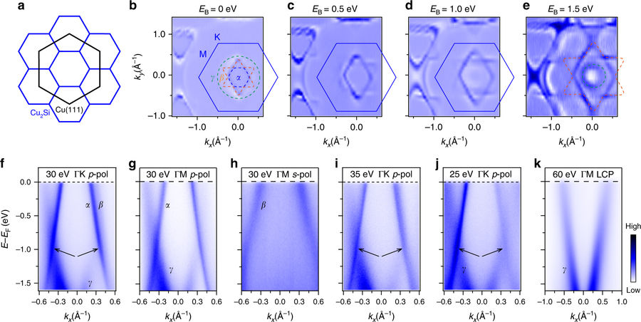
Figure 2 ARPES results for monolayer Cu2Si on Cu(111). a Schematic drawing of the Brillouin zones of Cu2Si (blue hexagons) and Cu(111) (black hexagon). As the lattice of Cu2Si is R30° with respect to the Cu(111)-1 × 1 lattice, the K point of Cu(111) is located at the Γ point of the second Brillouin zone of Cu2Si. b–e Second derivative CECs measured using 30-eV p-polarized photons. Three closed contours have been observed: a hexagon, a hexagram, and a circle, as indicated by the dashed lines. f, i, j ARPES intensity plots along the Γ-K direction measured with different photon energies: 30, 35, and 25 eV, respectively. The black arrows mark the position of the crossing points. g, h ARPES intensity plots along the Γ-M direction measured with p and s polarized light, respectively. k ARPES intensity plots along the Γ-M direction measured with 60-eV circularly polarized light. The γ band is clearly observed while the α and β bands are suppressed
Topological nodal line semimetals, a novel quantum state of materials, possess topologically nontrivial valence and conduction bands that touch at a line near the Fermi level. The exotic band structure can lead to various novel properties, such as long-range Coulomb interaction and flat Landau levels. Recently, topological nodal lines have been observed in several bulk materials, such as PtSn4, ZrSiS, TlTaSe2 and PbTaSe2. However, in two-dimensional materials, experimental research on nodal line fermions is still lacking. Here, we report the discovery of two-dimensional Dirac nodal line fermions in monolayer Cu2Si based on combined theoretical calculations and angle-resolved photoemission spectroscopy measurements. The Dirac nodal lines in Cu2Si form two concentric loops centred around the Γ point and are protected by mirror reflection symmetry. Our results establish Cu2Si as a platform to study the novel physical properties in two-dimensional Dirac materials and provide opportunities to realize high-speed low-dissipation devices.